

For a 3-pin device, during each switching cycle (turn-on or turn-off), the stray inductance of the source wiring combined with the slope of the switching current generates a voltage signal opposite to the MOSFET gate drive voltage (VGS). This voltage signal slows down the switching speed and increases switching losses in each cycle.The introduction of the Kelvin source isolates the gate drive network referenced to the Kelvin source from the power path. In this scenario, the drive signal remains free from interference caused by large, rapidly changing currents in the power path. The outcome is reduced total power loss of the transistor, lower operating temperature, and a more reliable, longer-lasting power supply system.
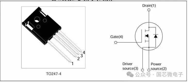
Figure 1. Package and Electrical Symbol (4-Pin)
Introduction to TO‑247‑3 and TO‑247‑4 Package Types
The MOSFET in TO‑247‑3 package is shown in Figure 2. It generally has three pins: gate, drain and source. For the TO‑247‑3 package, the gate drive loop and power loop share the source pin. A MOSFET is a voltage-controlled switching device. Its turn-on and turn-off behavior is determined by the voltage applied between the gate and source terminals, commonly referred to as VGS.
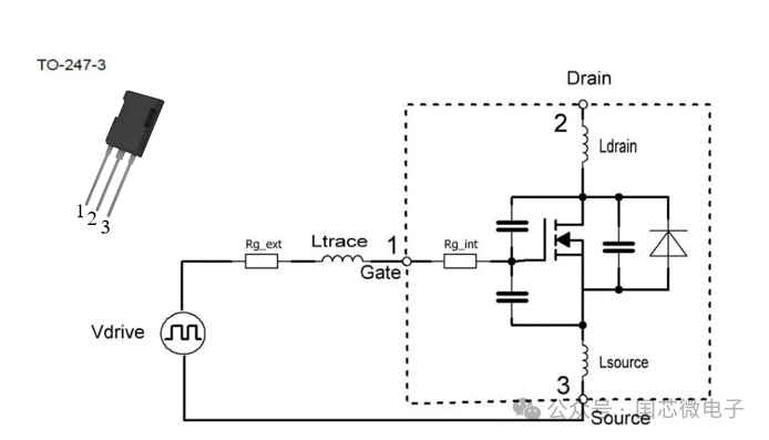
Figure 2 Traditional TO-247-3 Packaged MOSFET
From the model in Figure 2, several parameters deserve special attention as they exert a significant impact on the turn-on and turn-off behavior of the device. Rg_ext refers to the external resistor that users can employ to adjust the turn-on and turn-off of discrete devices. Rg_int is the internal gate resistance of the chip, and the sum of the two is known as the gate resistance of the device. The stray inductance of the gate loop, Ltrace, is introduced during PCB layout of the drive circuit, while the stray inductance Lsource is the parasitic inductance from the source package pin to the chip interior. The parasitic inductance Ldrain from the drain to the backside of the chip is not part of the drive loop and therefore excluded from this analysis.
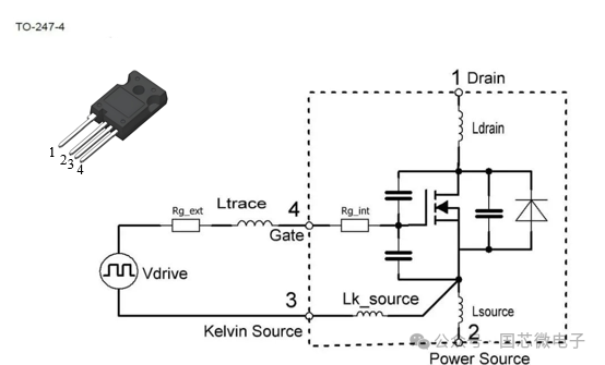
Figure 3 New TO-247-4 Packaged SiC MOSFET Model
The model of SiC MOSFET with TO‑247‑4 package is shown in Figure 3. We can see major changes in the pin count and pin definition of this package. Compared with TO‑247‑3, TO‑247‑4 has an additional auxiliary source pin, also known as the Kelvin pin. Meanwhile, this package decouples the gate drive loop from the main power loop, which facilitates the layout design of the drive board.
Data Analysis: Influence of Different Pin Counts on Switching Losses at Equal Power
(1) As shown in Figure 4, the red bar represents the switching loss of the 3-pin device. Under identical power conditions, the 4-pin device achieves lower loss. As power and current rise, the benefits of the 4-pin solution become more significant. Specifically, the reduction in turn-on loss is consistently maintained, and the decrease in turn-off loss becomes more pronounced with rising power. Therefore, the new solution delivers advantages across the full power range. As the market continuously pursues energy-saving solutions, this package enables new targets for heat dissipation and efficiency.
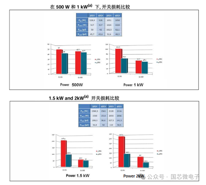
Figure 4. 3-Pin vs 4-Pin Switching Loss Comparison
Benefits of the TO-247-4 Auxiliary Source Pin
Take IV1Q12080T3 (TO‑247‑3) and IV1Q12080T4 (TO‑247‑4), the typical 1200 V, 80 mΩ SiC MOSFET products released by Zhanchip Electronics, as examples. This section theoretically explains the technical logic of the auxiliary source pin in the TO‑247‑4 package and the difference in switching losses between the two packages.
(1) Turn-on Process Analysis
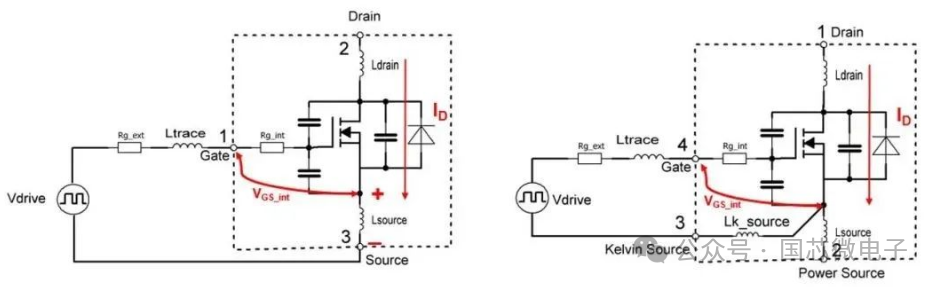
Figure 5. MOSFET Turn-on Analysis
During the turn-on process of the MOSFET device, its model is shown in Figure 5, and the mathematical model is as follows:
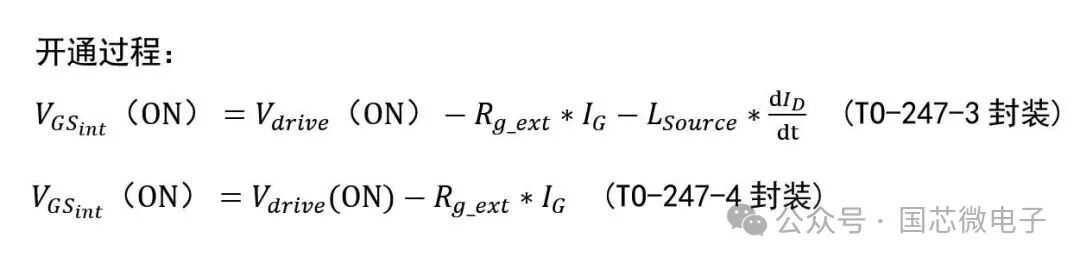
Take the TO‑247‑3 package as an example. During the MOSFET turn‑on process, the drain current ID rises rapidly. The high current slew rate generates a positive voltage drop across the power source stray inductance Lsource, expressed as LSource*(dID)/dt (positive at the top, negative at the bottom). This voltage drop means that the internal gate voltage VGS_int on the MOSFET chip does not equal the drive voltage at the very instant of turn-on; instead, it is reduced by the voltage developed across Lsource. The gate voltage is therefore lower at the turn-on instant, which slows the rise rate of ID and increases Eon. For IV1Q12080T4 (TO‑247‑4), no large current flows through the gate loop, so there is no disturbance from the main power path. The chip gate can correctly sense the drive voltage. Consequently, IV1Q12080T4 (TO‑247‑4) delivers lower turn-on loss compared with IV1Q12080T3 (TO‑247‑3).
(2) Turn-off Process Analysis
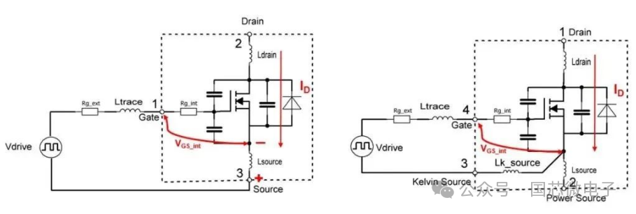
Figure 6. MOSFET Turn-off Analysis
During the turn-off process of the MOSFET device, its model is shown in Figure 6, and the mathematical model is as follows:
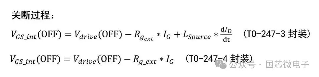
Take TO‑247‑3 as an example. During the MOSFET turn‑off process, the drain current ID drops rapidly. The high current slew rate creates a negative voltage drop across the power-source stray inductance Lsource: LSource*(dID)/dt (negative at the top, positive at the bottom). This voltage offset means that the internal gate voltage VGS_int on the MOSFET chip does not match the drive voltage at the instant of turn-off; instead, it is boosted by the voltage generated over Lsource. As a result, the gate voltage decays slowly at turn-off, which slows the fall rate of ID and raises Eoff. For IV1Q12080T4 (TO‑247‑4), no large current flows through the gate loop, so there is no disturbance originating from the main power path. The chip gate can correctly sense the drive voltage. Therefore, IV1Q12080T4 (TO‑247‑4) also achieves lower turn‑off loss compared with IV1Q12080T3 (TO‑247‑3).
Summary
The SiC MOSFET in TO‑247‑4 package incorporates an auxiliary source pin, which eliminates the shared source connection between the gate drive loop and the power loop and achieves decoupling of the two loops. Meanwhile, since the TO‑247‑4 packaged switching device suffers no gate voltage attenuation caused by the power source, the SiC MOSFET (TO‑247‑4 package) features faster switching speed and lower switching losses compared with the TO‑247‑3 version.


official account
Some pictures on this website come from the Internet. If copyright issues are involved, please delete them according to the contact information published on the website.